N5ESE's Outboard T/R Switch
For QRP "Separates"
(click on any picture to see larger version)
I normally don't post projects of immature design here. But I originally built this in February of 2006 and simply haven't had the time to tweak it to perfection. Almost a year after it's initial testing, it still sits on the back of the bench. Sigh. I wouldn't hesitate to use it on-the-air, but I'd nonetheless welcome others to duplicate and/or modify it, especially so as to improve the on/off ratio of the T/R switch itself. Let me know how it goes...First Things First
I didn't originally realize it, but the more I think about it, the more I think the idea for this grew out of some discussions I had with my friend Dan Tayloe, N7VE. Aside from being a die-hard homebrewer like myself, Dan is an accomplished and recognized RF Engineer. In fact, a circuit eerily like this is used in some designs (like the NC2030 and the FireFly transceivers) that were engineered by him more than a year before I slapped mine together. At any rate, I'd like to publicly thank Dan Tayloe, N7VE and Steve Weber, KD1JV, for the many ways they have inspired my own homebrewing adventures, as well as for the myriad ways they have enriched the experience of homebrewers and kit builders in the QRP community at large. To both - Salud!
A New T/R Switch Idea?
There are a lot of discrete tramsmitter and receiver circuits out there, in print and on the Internet, targeted at the QRP builder. Alas, these "standalones" rarely address the transmit/receive issue adequately. I remember a few years ago, eager to test my "Altoobs" design, and swapping BNC cables back and forth to switch between transmit and receive, and enduring unbelievably loud sidetone in an unmuted receiver. It's not that the receiver was incapable of muting - it was that I didn't prepare a suitable T/R circuit for it.
The project I present here is my attempt at a universal QRP T/R switch. The idea is to take care of the essentials, so that any QRP (i.e., less than 10W) receiver ***AND*** CW transmitter can be connected, and work seamlessly. These are what I considered the "essentials" to be:
- The transmitter RF Output is always connected to the antenna (i.e., not switched);
- The T/R Switch switches the receiver OUT of the transmit (antenna) circuit;
- The T/R Switch protects the receiver from excess signal during transmit
- The T/R Switch accepts the key input;
- The T/R Switch keys the transmitter;
- The T/R Switch provides a mute signal for the receiver;
- The T/R Switch provides a sidetone signal for the receiver;
- The T/R Switch provides all sequencing for full and automatic QSK (break-in) CW;
- The T/R Switch is independently powered, and efficiently so.
The operational scenario would be as follows, and could easily be applied to any QRP transmitter (or transceiver used as a transmitter) and any receiver (or transceiver used as a receiver). But the device is especially designed to accommodate a simple transmitter and receiver, each having few embellishments, and requiring none. Operationally, here's how a typical case would work:
- Using a "tee", connect the T/R Switch to the Transmitter-Antenna Coax (50-ohms)
- Connect the Receiver Input (i.e., antenna) via coax to the T/R Switch
- If the receiver has a "Mute" input, connect it to the T/R Switch
- If the receiver has a "sidetone" or "aux audio" input, connect it to the T/R Switch
- Connect the key (any type) to the T/R Switch
- Connect the T/R Switch "key out" to the transmitter's "key in"
- Power the T/R switch (9-Volt Battery)
- Operate at will
Nice, But How Are We Going To Do It?
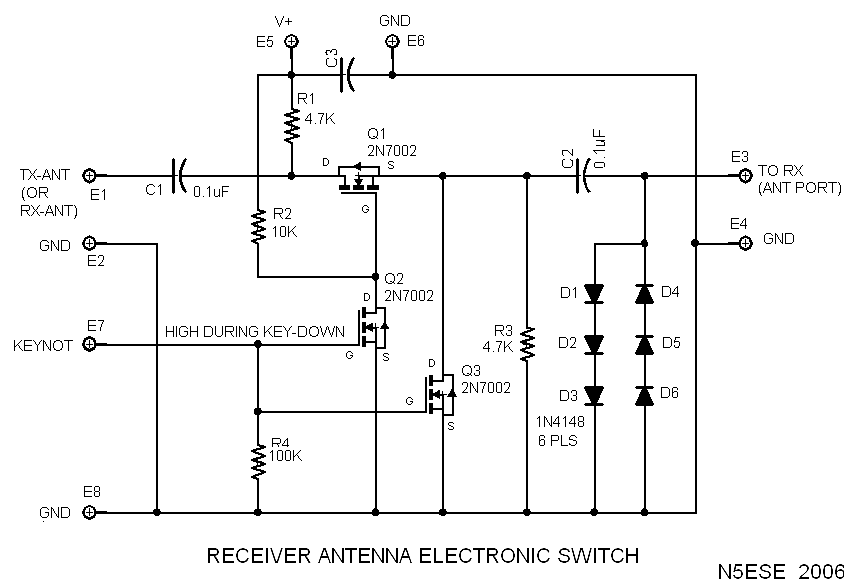
When Steve Weber, KD1JV, used three 2N7000 power MosFETs in the final of his AT Sprint transceiver, and managed to produce 6 watts with same (4W at 20 Meters), it really opened my eyes to these little devices. I had always thought of these as audio or power-control devices, but now I began to think in a different direction. One thing that immediately occured to me is that these devices might be configured in such a manner as to provide an "on/off" switch to RF energy between the transmit line and the receiver's antenna input. They could additionally provide protection to the receiver, by shunting any unwanted energy that might make it as far as the receiver's antenna input. This led to some experimenting in SPICE, and eventually to the following essential T/R switch circuit:
(click on the above image to see a higher-res version)Let's review the schematic. The transmit signal is tapped at the transmitter output - the transmitter remains connected to the antenna at all times - and arrives at the left "TX-ANT" port. Q1 serves to connect the receiver antenna port (right, "TO RX") to the antenna (during receive), or isolate it (during transmit). Because Q1 does not completely isolate the transmit signal (because of device leakage), Q3 serves to short the receiver input during transmit. The array of diodes clips any signals that may arrive during receive periods, and limits any voltage presented to the receiver antenna input to about 4 Volts peak-to-peak. Q2 is the control buffer for Q1. A "high" control signal to the "KEYNOT" port (from the control circuitry, representing the "key-down" i.e., transmit condition) ) causes Q2 to turn ON, Q1 to turn OFF, and Q3 to turn ON. Conversely, a "low" control signal (the key-up/receive condition) causes Q2 to turn OFF, Q1 to turn ON, and Q3 to turn OFF.
I won't belabor the details of the SPICE analysis, but you can see at least partial results in a whitepaper -here-. The challenge, for those of you who are interested in improving the circuit, is to improve the OFF condition, so that it really does isolate the receiver from the transmit line, all without significantly affecting the transmit impedance or transmit power. In real world measurements, at 30 Mhz, we are only seeing about 18 dB of isolation. Lower frequencies are considerably better, on the order of 30-36 dB.
Another challenge is to protect the switch itself (Q1) from high voltage due to high SWR (for example, from transmitting into a bad mismatch or missing antenna). I've not yet encountered that condition, but it could potentially be catastrophic to Q1. Avoid the temptation to protect it with a zener, as the capacitance in the zener may actually degrade the isolation further.
FLASH! Dan Tayloe, N7VE, suggests the BSS123 as a substitute for the 2N7002. On reviewing the data sheets, it looks like it could add some much-needed design margin to the T/R Switch. With a Drain-Source rating of 100V (versus 60V for the 2N7002) and about half the capacitances, it should perform at least as well, and maybe even improve the isolation, to boot.
By the way, you may have noticed that the TX ANT port (left) is also labeled RX ANT. You are free to connect a separate receive antenna, and the device will still provide isolation from coupled energy.
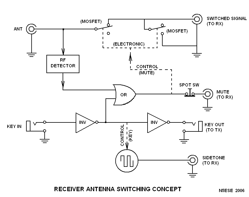
You've probably already noticed that a bunch of features that I listed earlier are not implemented in the above circuit. These are provided by the control circuitry. Here's a conceptual block diagram of what we are attempting to accomplish:
(click on the above image to see a higher-res version)Keep in mind, this is a functional, conceptual layout. The first thing you'll notice, in the upper right corner, are the RF switches, corresponding to Q1 and Q3, discussed earlier. The control signal for those switches (shown as dotted lines) is developed from one (or both) of two input signals: the keying input, and/or the RF detector. Normally, the keyline controls the condition of the RF switch circuit, but what would happen if the transmitter were keyed from a front panel switch, instead of from the key? The RF Detector would detect the presence of RF and immediately disconnect the receiver input.
The RF Detector also assures that the T/R Switch remains engaged for that few milliseconds after the key is released, in which the tranmitter is still producing RF. In fact, however long that takes, the RF Detector will keep the T/R Switch activated. On key-down, the keying circuit immediately activates the T/R Switch, before the Transmitter has actually generated RF. On key-up, however, the RF Detector makes sure the T/R switch stays activated. In this way, we don't have to create a complex sequencer to produce a particular on-delay and off-delay. This approach assures universal application without having to know the timing characteristics of a particular transmitter's keying circuit.
Two ancillary functions are provided by the control circuitry also. A keyed sidetone oscillator provides audio for injection into the receiver. In a typical simple receiver project, the addition of a resistor at the audio amplifier input is all that is required to add an auxiliary audio input. Many older commercial receivers already have such an input (as well as a "ground to mute" input). Lastly, a spot function is provided to disable the mute so that the actual transmit signal can be monitored, for zero-beating.
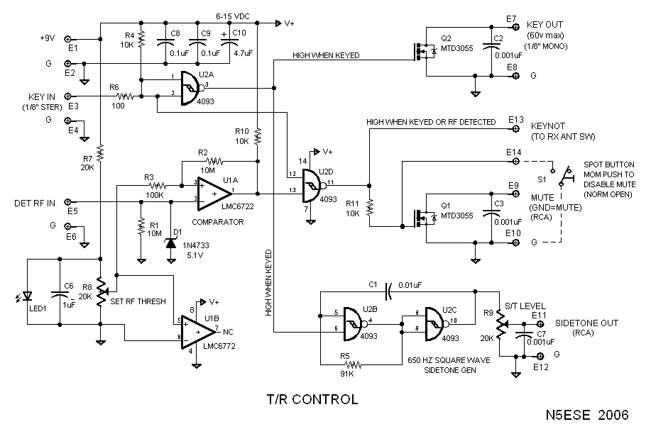
And here's the actual control circuit:
(click on the above image to see a higher-res version)In the schematic above, NAND Gate U2D serves to "OR" the keyline and detected RF to drive power mosfet Q1, our muting switch. The mute signal is an output to the receiver, optionally used, which provides a ground when the transmitter is expected to be active. The signal which drives transistor Q1 also gets routed to the KEYNOT control input on the RF Switch board, activating those switches to the "transmit" condition (thereby isolating the receiver from the antenna).
NAND Gate U2A serves to buffer the keyline, and drives our output keying transistor Q2, which keys the transmitter. U2A also keys our Sidetone Generator, a 650 Hz relaxation oscillator formed from U2B, U2C, C1, and R5. A trimmer pot R9 allows us to adjust the sidetone level to a level suitable for our particular receiver.
From an external board (RF Detector Board), a DC signal representing transmit RF voltage level is applied to an analog comparator (U1A and supporting circuitry). This circuit compares that DC level (from the RF Detector) to the level set by R8, which is a portion of the reference level set by LED1 (used here like a 2 Volt zener diode). The comparator is capable of detecting milliwatt levels of RF, and upon detection, sends that signal to our OR gate U2D. In this way, we provide a level of protection for the receiver against inadvertant transmit power, and even energy coupled into the receive antenna when the receiver uses a separate antenna.
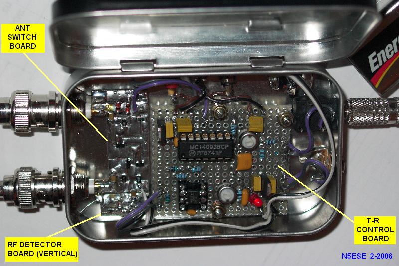
The total functionality is proviided on 3 boards (in this particular incarnation): A control board, the RF switch board, and an RF detector. This mainly reflects the evolution of the project, although there may be some design merit to removing the control circuitry from the vicinity of the RF Switch board and any circulaing ground currents that might exist there.
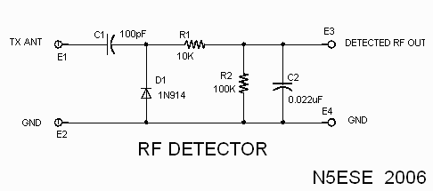
Below we see the RF Detector circuit, a small board placed in close proximity to the transmit antenna port. It functions like a classic RF Probe (diode detection method):
Construction
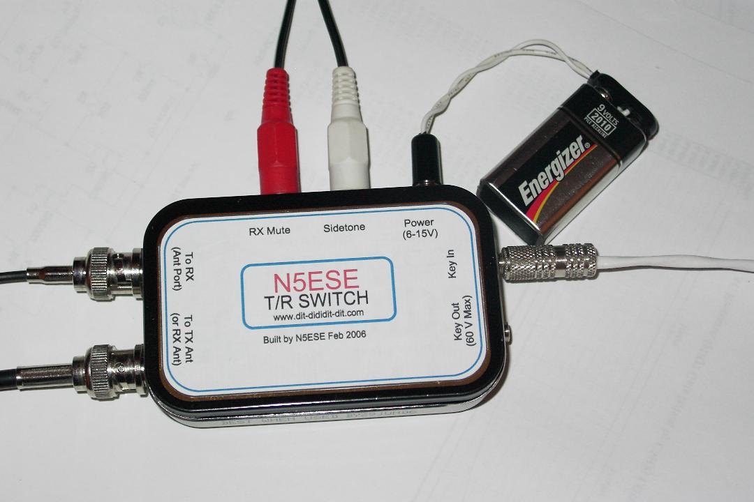
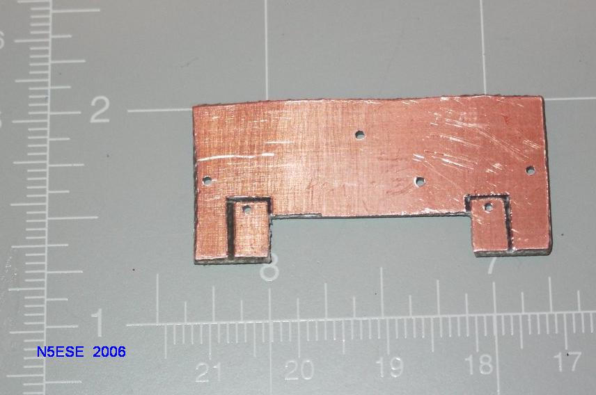
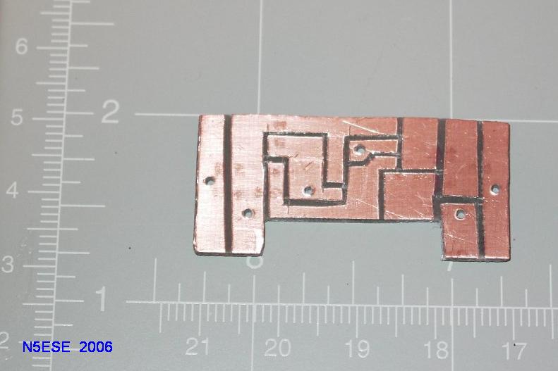
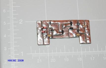
The Altoids tin provides the ideal compact, shielded assembly we need in this application. Unfortunately, using the prototyping methods chosen, we could not fit the 9 Volt battery inside, so that ends up "hangin' out". The two antenna connectors (BNC types) were mounted on one end of the box, and the RF Switch board was designed specifically to fit compactly between those two connectors, so as to minimize any stray RF fields or circulating ground currents that might introduce themselves into the control circuitry. The method also allows us to maximize OFF isolation and minimize ON resistance at RF frequencies. But to accomplish the small assembly, surface mount techniques were used ("cut-and-peel" fabrication methods). Here are some pictures of the RF Switch PCB, top and bottom, before mounting components:
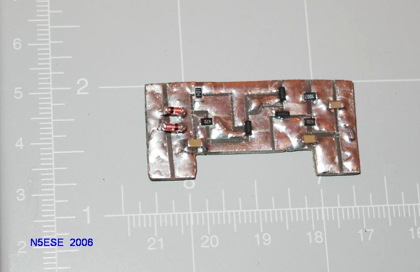
(click on the above image to see a higher-res version) And here's a picture of the RF Switch assembly, after mounting components, but before installing in the Altoids tin:
(click on the above image to see a higher-res version)The RF Detector board was also built "surface mount" ugly style, on a small piece of scrap board. Control circuitry was built on a piece of scrap perf board. See the picture below:
(click on the above image to see a higher-res, annotated version)Hooking It Up
To hook it up, if the transmitter and receiver are to share one antenna:
To hook it up, if using separate transmit and receive antennas:
- Connect a "Tee" at the "TX-ANT" port of the T/R Switch
- Connect a short piece of coax from the tee to the transmitter
- Connect another short piece of coax to the antenna tuner (or 50-ohm antenna)
- Connect a short piece of coax from the "RX-ANT" port of the T/R Switch, to the Receiver's antenna input jack.
- Connect a shielded cable from the key (or keyer) to the KEY-IN port of the T/R switch
- Connect a shielded cable from the KEY-OUT port of the T/R switch to the "key" input on the Transmitter (note: positive keying only, maximum 40V)
- If a "ground-to-mute" input is available on the receiver, connect a short piece of shielded cable from that to the MUTE port of the T/R switch
- If an "aux audio" (or "sidetone") input is available on the receiver, connect a short piece of shielded cable from that to the S/T port of the T/R switch
- Assure 9-Volt power applied to the T/R Switch
- Adjust your Antenna Tuner at low power (1 watt or less), or use a resistive bridge for tuning (or pre-tune the antenna)
- Operate at will!
- Connect the transmitter to its antenna system as usual
- Connect the receive antenna to the TX-ANT port on the T/R Switch
- Connect a short piece of coax from the "RX-ANT" port of the T/R Switch, to the Receiver's antenna input jack.
- Connect a shielded cable from the key (or keyer) to the KEY-IN port of the T/R switch
- Connect a shielded cable from the KEY-OUT port of the T/R switch to the "key" input on the Transmitter (note: positive keying only, maximum 40V)
- If a "ground-to-mute" input is available on the receiver, connect a short piece of shielded cable from that to the MUTE port of the T/R switch
- If an "aux audio" (or "sidetone") input is available on the receiver, connect a short piece of shielded cable from that to the S/T port of the T/R switch
- Assure 9-Volt power applied to the T/R Switch
- Adjust your Antenna Tuner as you normally would
- Operate at will!
Observations
I tested the circuit at 1W, 5W, and 10 Watts, using a K2 and external antenna tuner, pre-matched to 50-ohms. For the receiver, I used an old 70's vintage Heatkit HR-1680, which has both a mute and sidetone inputs.
80, 40, and 20 Meters performed flawlessly, and I made a few QSOs on 40M. On 15 and 20M, I began to see an affect on SWR, but it was still usable. When I removed the MUTE control, a significant amount of RF could be heard in the receiver (and observed on the S-Meter.
QSK (break-in) was in the neighborhood of 20-25 wpm, and receiver performance was not noticeably different than if it were hooked directly to the antenna. The RF detector was verified to protect the receiver, even if the transmitter was tuned without a key. Keying performance was as expected. With a separate antenna, the RF Switch isolation was sufficient even on the higher bands.
Subsequent tests on the bench revealed that the RF Switching was not providing the degree of isolation anticipated as a result of SPICE simulations. OFF isolation was seen to be about 18 dB at 30Mhz, increasing to about 36 dB at 4 Mhz. This leaves some considerable room for improvement, and I invite any suggestions. Still, the isolation is quite adequate for use on frequencies 14 MHz and lower, and still "usable" at the higher frequencies.
The 2N7000 switch has a maximum drain-source specification of 60V. While this corresponds to a transmitter power of 35 Watts in a 50-ohm antenna circuit, it only corresponds to a power of about 1-1/2 Watts for a 1000-ohm circuit. Therefore, the device is susceptible to catastrophic failure if it is connected to a badly mis-matched transmitter/antenna, even at QRP power levels. In using the T/R switch, then, it is wise to first adjust your antenna tuner for a good match at reduced power, and then raise the power to normal operating levels (but still no more than 10 watts). Alternatively, use an antenna tuner with a resistive bridge circuit, such as the Norcal BLT, because it provides a maximum mismatch of about 2:1 to the transmitter (when in the "Tune" mode).
As an added benefit, the T/R switch draws very little power in the quiescent (receive) state, meaning that the 9-Volt battery lasts a long, long time (I'm not sure how long, but I left mine connected for weeks at a time).
Conclusion
I think this is a useful gadget to have for anyone who likes to build QRP "separates". I'd heartily welcome suggestions that might result in improved performance, while retaining its "universal" application.
73,
Monty N5ESE
dit dididit dit
Return to N5ESE home page
Overseer: Monty Northrup ...... leave e-mail ...